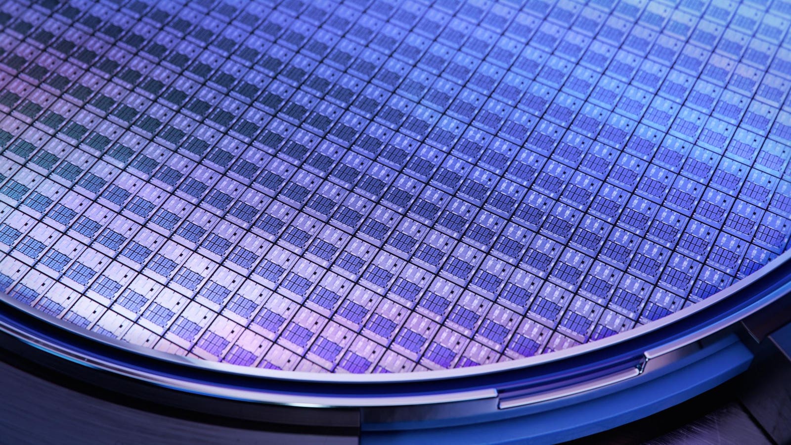
This is another article on some interesting developments from the IEEE Hot Chips Conference at Stanford, but first some interesting semiconductor statistics on industry equipment purchases and semiconductor sales. Continuing these trends could drive the use of NVIDIA networking and interconnect products and a Google Ironwood TPU technology for sharing 1.77PB of High bandwidth memory, HBM.
The Semiconductor Industry Association, SIA, announced global semiconductor sales were $62.1 billion during the month of July 2025, an increase of 20.6% compared to the July 2024 total of $51.5 billion and 3.6% more than the June 2025 total of $59.9 billion.
Regionally, year-to-year in July sales were up in the Asia Pacific/All Other (35.6%), Americas (29.3%), China (10.4%), and Europe (5.7%), but decreased in Japan (-6.3%). Month-to-month sales in May increased in the Americas (8.6%) and Asia Pacific/All Other (4.9%), remained steady in Europe (0.0%), and declined in Japan (-0.2%) and China (-1.3%). The chart below shows WSTS tracking of overall semiconductor revenue and year-over-year percent changes.
WSTS Worldwide Semi revenues and trends
SIA
Making the latest generation of semiconductors takes capital investment and a big part of that investment is in equipment. SEMI reports that, global semiconductor equipment billings increased 24% year-over-year to US$33.07 billion in the second quarter of 2025. Second quarter 2025 billings registered a 3% quarter-over-quarter expansion supported by the leading-edge logic, advanced high bandwidth memory (HBM) related DRAM applications, as well as increase in shipments to Asia. The chart below shows where these investments are being made.
Semi equipment spending trends
SEMI
In particular, China and Taiwan led in equipment purchases with Taiwan more than doubling its spending from the prior year. North American equipment purchases were modestly higher than a year ago.
The semiconductor industry and the equipment that support that industry are showing robust continuous growth in most parts of the world supporting consumer, industrial and data center applications. The Hot Chips Conference had a particular focus on data center semiconductor developments, including several from Nvidia. At the event Nvidia speakers particularly focused on enterprise inference applications, where AI hopes to achieve its return on investment as pointed out in the slide image below.
Putting AI inference at enterprise scale
Nvidia
Communication within chips and between chiplets and within and between data center racks saw some interesting Nvidia announcements, including the introduction of its Spectrum-XGS Ethernet for supporting distributed AI between remote data centers to create what Nvidia says, will be the world’s largest supercomputers.
Nvidia Spectrum XGS Ethernet
Nvidia
The company also spoke about NVLink Fusion, a rack-scale scale up fabric, shown in concept below.
Nvidia and others at Hot Chips also talked about co-packaged optics built into switch ASICs to provide high bandwidth and low latency that can be used to connect millions of GPUs. With faster connections between GPUs and memory, with and between racks and between data centers Nvidia projected ambitious plans to create high performance AI training and inference.
Another interesting presentation focused on memory included the discussion by Google of their Ironwood TPU chips which use optical circuit switches, OCSs, to share HBM memory of 1.77PB. The slide below shows this memory sharing which includes significant redundancy in data placement to deal with deal with bad data in individual memories.
Google Ironwood TPU memory sharing
Semi sales & capital spending is up from last year. Continuing this trend may depend upon networking and interconnect technologies from the 2025 Hot Chips Conference.


